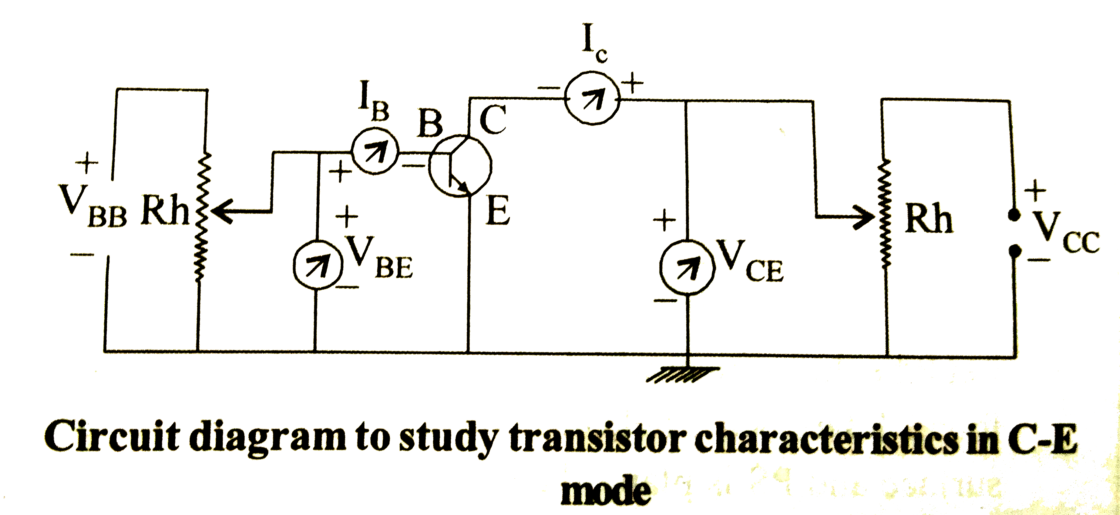
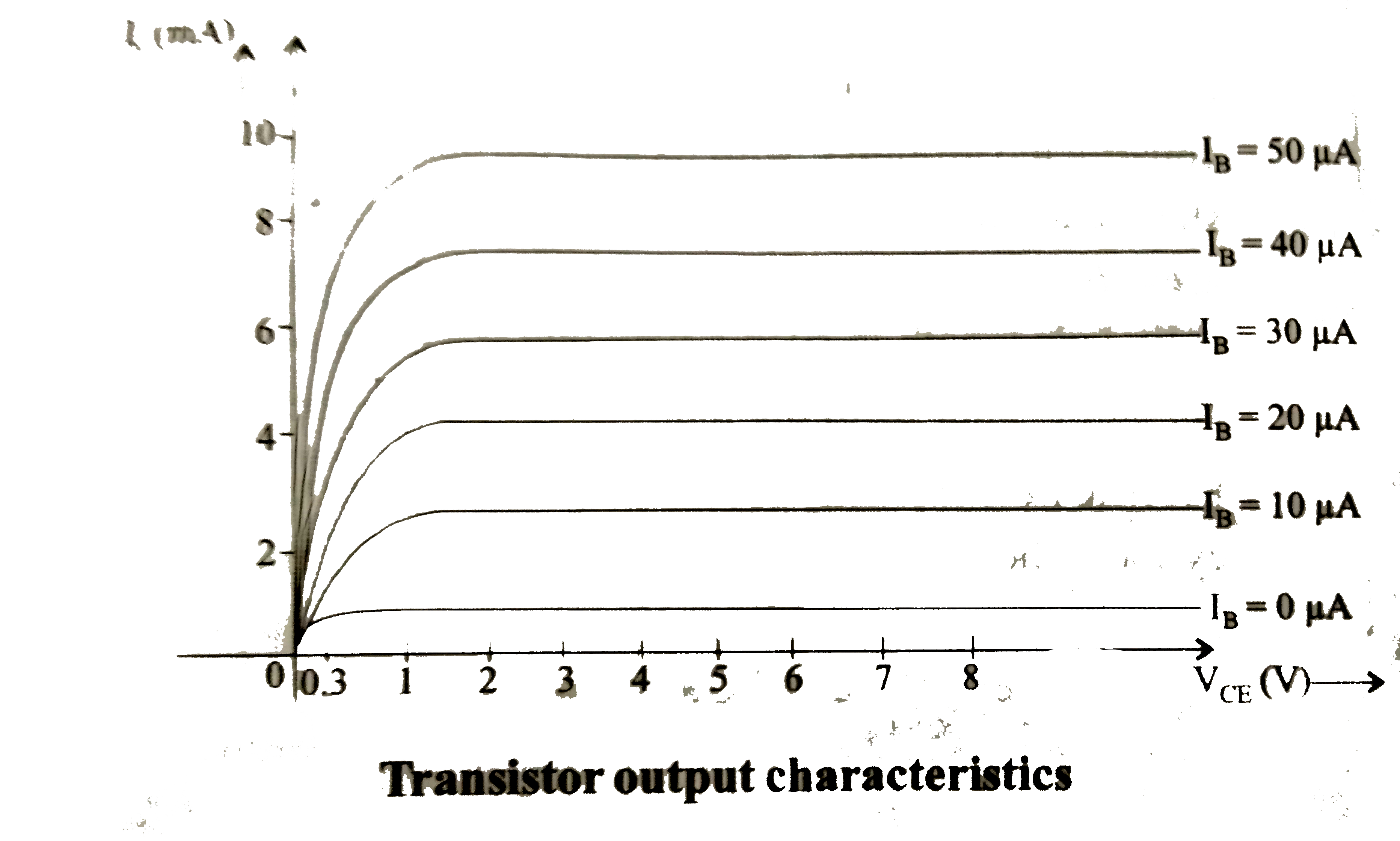
For Collector-Emitter mode, it is a graph of collector current `(I_(c))` versus collector voltage `(V_(CE))`, for the fixed value of the base courrent. For output charateristics,`I_(B)` is kept constant `V_(CE)` is increased in small steps and `I_(C)` is recorded at every step.
From output characteristics, it is observed that
(i) When `I_(B)=0,I_(C)` is nearly zero, hence the trasistor is an cut off region.
(ii) For `V_(CE)lt0.3V,I_(C)` increases with `V_(CE)` and can be controlled by `V_(CE)`,
(iii) When `V_(CE)gtV_(BE)gt0.7V,C-E` jnuction gets reverse baised and `I_(C)` gets saturated, hence the transistor is in active reagion.
When `V_(CE)lt0.2V`, both the junctions get forward biased and `I_(C)` can no longer be controlled by `V_(CE)`, hence the transistor is the saturation region.
The dynamic output resistance of transistor is
`r_(0)=((DeltaV_(CE))/(DeltaI_(C)))_(I_(B)" is constant")`
In C-E mode, output resistance varies from few `KOmega` to `KOmega`.


