Use app×
Join Bloom Tuition
One on One Online Tuition
JEE MAIN 2025 Foundation Course
NEET 2025 Foundation Course
CLASS 12 FOUNDATION COURSE
CLASS 10 FOUNDATION COURSE
CLASS 9 FOUNDATION COURSE
CLASS 8 FOUNDATION COURSE
0 votes
2.7k views
in Physics by (150k points)

Draw the circuit arrangement for studying the input and output characteristics of n-p-n transistor in CE configuration. 

Draw the typical nature of these input and output characteristics. Explain how these are obtained. 

Define the terms (i) input resistance and (ii) current amplification factor

1 Answer

0 votes
by (87.4k points)
selected by
 
Best answer

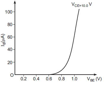
Input characteristics: The variation of the base current Ib with the base-emitter voltage Vbe at constant Vce. Input characteristics can be drawn, when the transistor is in active state, so Vce is kept enough large. So base collector junction remain in reverse biased mode i.e., Vce >> 0.7V. 

Output characteristics: Output characteristic is obtained by measuring the collector current IC with the variation in Vce keeping base current Ib constant. Input resistance: It is defined as the ratio of change in base - emitter voltage Vbe to the resulting change in base current Ib at constant Vce.

Current Amplification: It is defined as the ratio of change in collector current IC to the change in base current Ib at a constant Vce, when the transistor is in active state.

βac = (ΔIc/ΔIb)

Welcome to Sarthaks eConnect: A unique platform where students can interact with teachers/experts/students to get solutions to their queries. Students (upto class 10+2) preparing for All Government Exams, CBSE Board Exam, ICSE Board Exam, State Board Exam, JEE (Mains+Advance) and NEET can ask questions from any subject and get quick answers by subject teachers/ experts/mentors/students.

Categories

...